To understand how a PC boots, you need to dive into Real Mode — the operating mode every x86 processor wakes up in, since the 8086 in 1978. This article explains, using the Compaq Deskpro XE 466 (486, circa 1994) as a concrete example, how the BIOS brings a machine to life: from the very first instruction after power-on to loading the operating system.
Real Mode: The Basics
In Real Mode the CPU operates in 16-bit mode. This means:
- Registers are 16 bits wide (AX, BX, CX, DX, SI, DI, BP, SP)
- The address bus is 20 bits wide → maximum 1 MB of addressable memory (0x00000–0xFFFFF)
- There is no memory protection, no paging, no privilege separation
- Any program can read, write, and execute any memory location
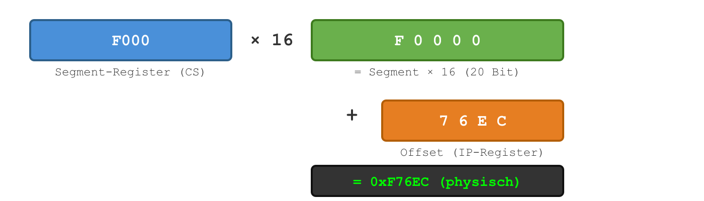
Segment:Offset Addressing
Because 16-bit registers can only address 64 KB (0x0000–0xFFFF), Real Mode uses a Segment:Offset scheme to reach the full 20-bit address space:
Physical Address = Segment × 16 + Offset
Example: F000:76EC → 0xF0000 + 0x76EC = 0xF76EC
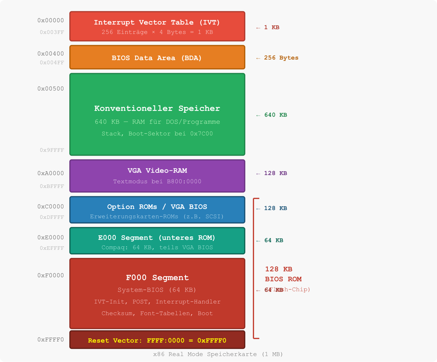
The 1 MB Memory Map
The entire 1 MB address space is divided into fixed regions. Here is the map as used by the Compaq Deskpro XE 466:
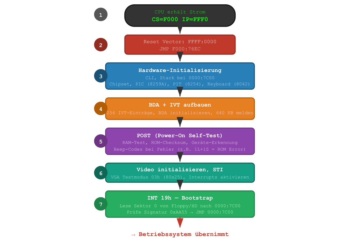
The Reset Vector: Where It All Begins
When an x86 processor receives power (or a reset signal), it always jumps to the same address:
FFFF:0000 → physical 0xFFFF0
That’s the last 16 bytes of the address space. There’s barely enough room for a short jump instruction — so the reset vector contains a FAR JMP to the actual BIOS entry point.
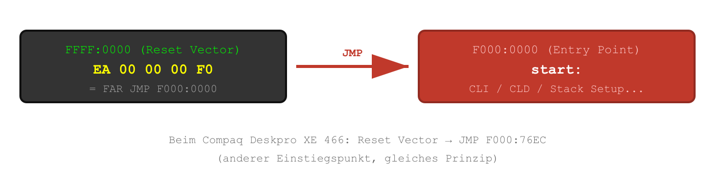
On the Compaq Deskpro XE 466, the reset vector contains JMP F000:76EC — that’s where the actual POST (Power-On Self-Test) begins.
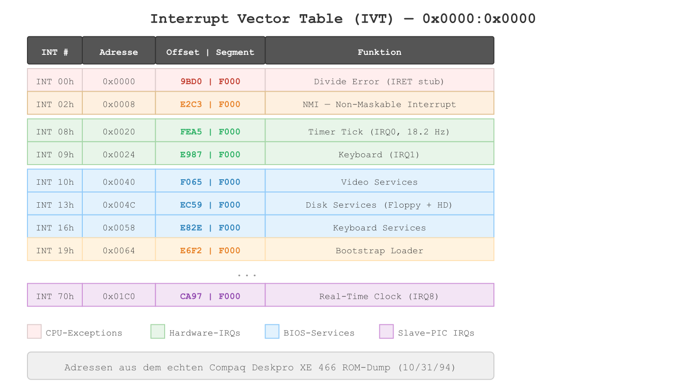
The Interrupt Vector Table (IVT)
The IVT is the central dispatch table of the Real Mode BIOS. It sits at the very beginning of memory at 0x00000–0x003FF and contains 256 entries — one for every possible interrupt (0x00–0xFF).
Each entry is 4 bytes: 2 bytes offset + 2 bytes segment → a FAR pointer to the corresponding handler.
How the BIOS Populates the IVT
The Compaq BIOS fills the IVT in 4 stages during POST:
- INT 20h–6Fh (80 entries) from an offset table at F000:FF43
- INT 60h–67h (8 entries) cleared to 0000:0000
- INT 70h–77h (8 entries) from a table at F000:FF33 (second PIC)
- INT 00h–1Fh (32 entries) from a table at F000:FEF3 (CPU exceptions + standard services)
A fascinating detail: the IVT offset table at F000:FF43 overlaps with the Print Screen handler at F000:FF54. The machine code bytes of the handler double as IVT offsets — a trick to save ROM space, but it means some interrupt entries point into the 8×8 font bitmap table instead of real handlers.
The BIOS Data Area (BDA)
Right after the IVT, at 0x0400–0x04FF, lies the BIOS Data Area — a 256-byte block where the BIOS stores runtime data:
| Offset | Size | Content |
|---|---|---|
| 0040:0010 | Word | Equipment flags (floppy present, video mode) |
| 0040:0013 | Word | Conventional memory in KB (640) |
| 0040:0017 | Byte | Keyboard shift flags (Ctrl, Alt, Shift, CapsLock) |
| 0040:001A | Word | Keyboard buffer head pointer |
| 0040:001C | Word | Keyboard buffer tail pointer |
| 0040:001E | 32 Bytes | Keyboard buffer (16 words, ring buffer) |
| 0040:0049 | Byte | Current video mode (03h = 80×25 text) |
| 0040:0050 | Word | Cursor position (column + row) |
| 0040:006C | DWord | Timer tick counter (18.2 Hz since midnight) |
The BIOS zeroes the entire BDA at startup and then sets the default values. Every interrupt handler reads and writes the BDA — it’s the shared „database“ between the BIOS and the operating system.
The Boot Sequence: From Power to OS
Key Components
8259A PIC — Programmable Interrupt Controller
Two cascaded 8259A chips route hardware interrupts (IRQs) to the CPU:
- Master PIC (port 0x20/0x21): IRQ 0–7 → INT 08h–0Fh
- Slave PIC (port 0xA0/0xA1): IRQ 8–15 → INT 70h–77h
- The slave is connected to the master on IRQ 2 (cascade)
8254 PIT — Programmable Interval Timer
Channel 0 is programmed to 18.2 Hz (divisor 65536). Each tick fires IRQ 0 → INT 08h, which increments the 32-bit counter in the BDA. 1,573,040 ticks = one day.
8042 Keyboard Controller
The keyboard handler (INT 09h) reads scancodes from port 0x60, translates them via lookup tables to ASCII, and writes the result into the BDA’s 16-word ring buffer.
The 128 KB ROM Layout of the Compaq
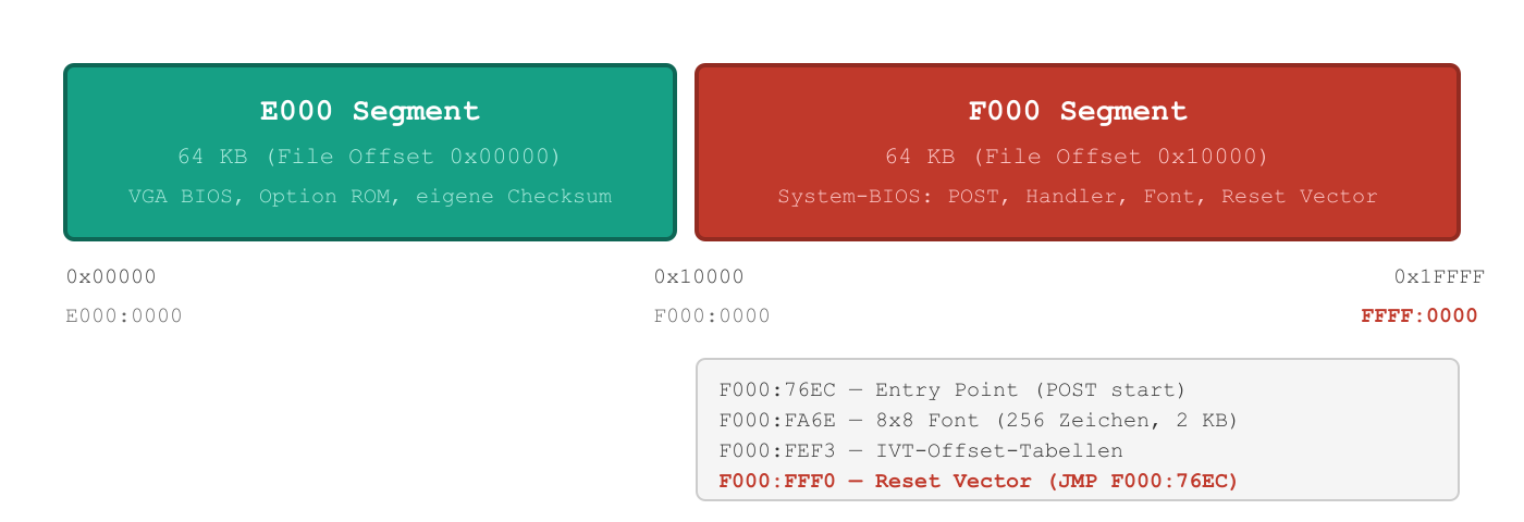
The 128 KB ROM is mapped as a single flash chip into the address range 0xE0000–0xFFFFF. The upper 64 KB (F000 segment) contains the actual system BIOS — including a byte-sum checksum that is verified during POST. A failure produces „101-ROM Error“ with one long + one short beep.
How an Interrupt Call Works
When software calls INT 10h (e.g., for screen output), the following happens:
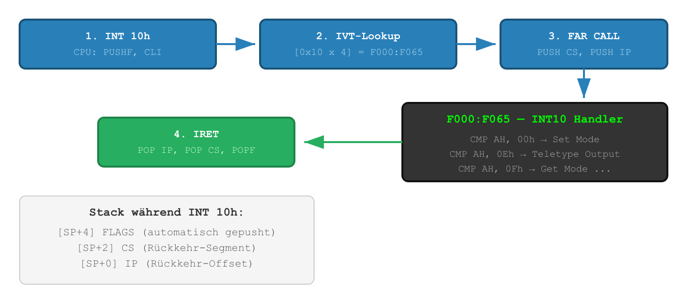
The CPU does three things automatically on INT n: push FLAGS onto the stack, disable interrupts (CLI), and FAR CALL to the handler. IRET (Interrupt Return) reverses everything.
Summary
| Concept | Details |
|---|---|
| Real Mode | 16-bit, 1 MB address space, no memory protection |
| Segment:Offset | Physical address = Segment × 16 + Offset |
| Reset Vector | FFFF:0000 (0xFFFF0) — first instruction after power-on |
| IVT | 256 × 4 bytes at 0x0000 — pointers to all interrupt handlers |
| BDA | 256 bytes at 0x0400 — runtime data (timer, keyboard, video) |
| POST | RAM test, checksum, hardware init, device scan |
| Boot | INT 19h → sector 0 to 0x7C00, check signature 0xAA55 → JMP |
| ROM Layout | 128 KB: E000 (VGA BIOS) + F000 (system BIOS + reset vector) |
All of these concepts have been in place since the original IBM PC in 1981 — and they work on the Compaq Deskpro XE 466 from 1994 exactly the same way as on a modern PC booting in Legacy BIOS mode. Real Mode is the common denominator of all x86 systems.
In the next article, I’ll show how we binary-patched this BIOS to support non-parity RAM — 19 patches, 24 bytes changed, and some hard lessons about bytes you’d better not touch.